Enroll in LiveTechINDIA’s PCB Design Course in Andheri, Mumbai and gain hands-on training to design industry-ready printed circuit boards. With expert-led sessions in Andheri and Panvel, this course helps you master PCB layout, signal integrity, and manufacturable designs using the latest tools—perfect for aspiring electronics engineers and hardware professionals.
(Is the founder of LivetechINDIA with 15+ years of experience in IT training, college partnerships, placement-driven learning, and IT career mentoring across Mumbai)


PCB Design in Mumbai offered by Livetechindia is the most popular course trained by industry trainers.
Our PCB Design course is your gateway to mastering the art of creating Printed Circuit Boards (PCBs) for electronic product development. Learn the principles, tools, and practices involved in translating schematics into manufacturing-ready layouts.
Gain hands-on experience with industry-standard PCB design tools, exploring signal integrity, power distribution, and manufacturability for efficient electronic systems.
Now learn PCB Design course training at Andheri. LivetechINDIA offers PCB Design certification at Mumbai.

")


Become a certified PCB Design expert with our specialized training program!
Trustindex verifies that the original source of the review is Google. Hi, this is Aayush, currently I'm a 3rd year Diploma Student at Agnel Polytechnic, vashi, I worked here as a intern, to be honest its been really a great experience where i had been learning so many new core concepts regularly with real industry based overview and the honorable mention Ms.Ravina Desai were a strong help throughout my internship period along with the Management Dept. of LivetechINDIA, truly enjoyed my time here, a proper guidance, clear problem solving within the scope of industry based realizational values thus developed projects related to PYTHON, NLP, POWERBI, and worked on Tenserflow, Matplotlib, Seaborn as well along with core concepts taught as mentioned in regards with the projects.Posted onTrustindex verifies that the original source of the review is Google. I’m currently doing my internship with LivetechIndia and the experience has been amazing so far. I started with Python basics and important libraries like Pandas and NumPy, taught by Ravina Desai ma’am — her teaching style is very clear and beginner-friendly, which made programming concepts easy to grasp. Later, I learned NLP and now Power BI from Mugdha ma’am. She explains each concept with practical examples and gives us hands-on tasks that really help in understanding the topics deeply. The environment here is positive, supportive, and motivating. Every doubt is solved with patience, and we get guidance for real-world applications as well.Posted onTrustindex verifies that the original source of the review is Google. It was an great Experience of learning python and power biPosted onTrustindex verifies that the original source of the review is Google. The overall teaching experience was very good. Special thanks to Mughda Ma’am for her excellent sessions on NLP, which were clear and easy to understand. The support and service during the internship were also good. However, there is room for improvement in the infrastructure of the classes, which would make the learning experience even better.Posted onTrustindex verifies that the original source of the review is Google. I recently completed my Data Analyst internship at Live Tech India, Thane. It was a great learning experience where I got hands-on exposure to real projects, data visualization, and analytical tools. The mentors were supportive, explained concepts clearly, and guided me throughout the training. I truly recommend Live Tech India for anyone looking to build a strong career in Data Analytics.Posted onTrustindex verifies that the original source of the review is Google. Good institute, amazing faculty, good classrooms.Posted onTrustindex verifies that the original source of the review is Google. The experience was good and I got so much to learn from this internship.Posted onTrustindex verifies that the original source of the review is Google. I recently completed my internship at [Livetech indian], and it was a great learning experience. I got to work with a helpful team and learned many new things.During my internship, I improved my skills.This internship helped me grow both professionally and personally. I now feel more confident and prepared for future job opportunities. Overall, it was a very useful experience, and I’m thankful for the opportunity.


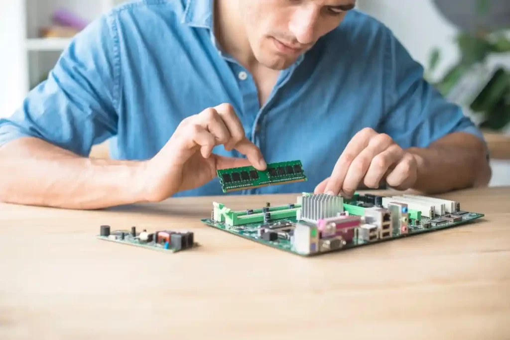
PCB Design involves creating the physical layout of a printed circuit board, translating a schematic into a format suitable for manufacturing. It includes considerations for component placement, signal routing, and manufacturing constraints.
Some PCB design tools offer free versions with limited features. However, professional-grade tools often require a paid license. Common tools include Altium Designer, Eagle, KiCad, and more.
Signal Integrity refers to the quality of electrical signals as they travel through a PCB. It involves minimizing distortion, noise, and interference to ensure reliable and accurate data transmission.
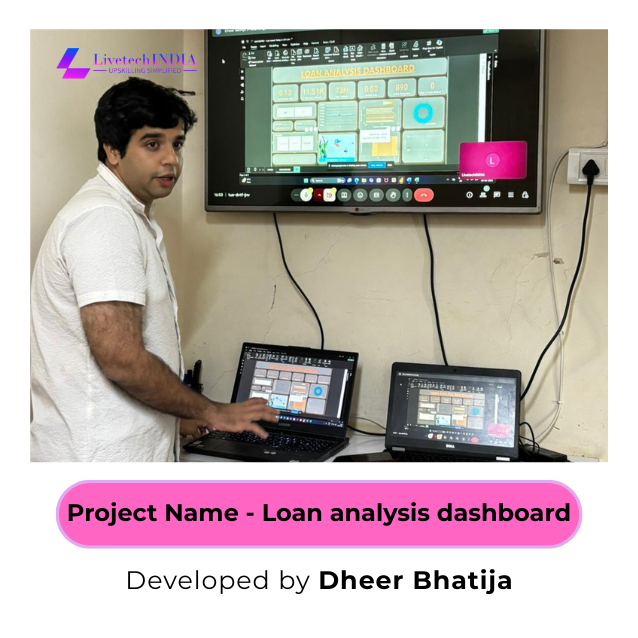
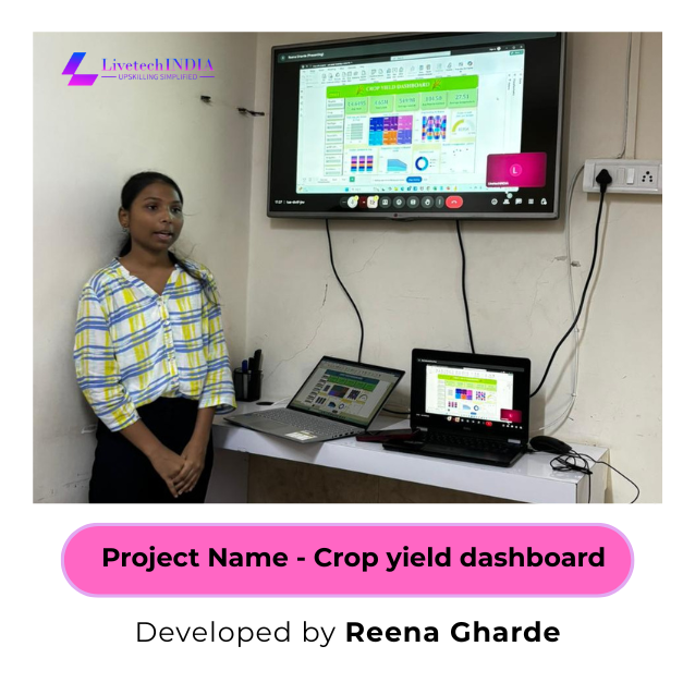
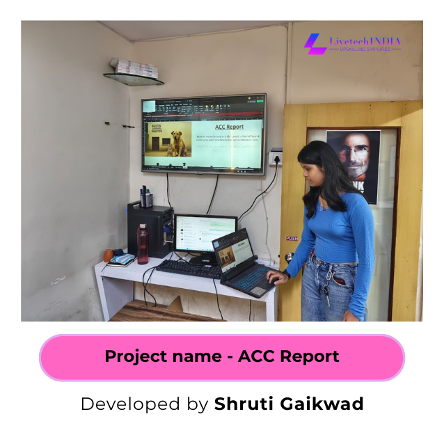
Yes, our students are making circuits in there projects. As entire training is practical, we give many tasks to perform.
Yes, the course will cover both fundamental and advanced PCB design techniques, including considerations for high-speed signals, multi-layer boards, and complex designs.
You can choose below delivery method according to your requirement:
LiveTechINDIA Training Center in Andheri offers one of the most comprehensive PCB Design Courses in Andheri, with hands-on training, expert instructors, and real-world projects.
LiveTechINDIA is widely recognized as a leading PCB Design Course Training Institute in Mumbai, offering beginner to advanced-level training, industry exposure, and placement support.
Yes, LiveTechINDIA provides dedicated placement support for all students completing the PCB Design Course in Andheri or Panvel, connecting them with job opportunities in the electronics and hardware design industry.
We offer flexible learning options including offline classes at our LiveTechINDIA Training Centers in Andheri and Panvel, and live online sessions for students across India.
No prior coding experience is required to start this course. Our syllabus is designed for complete beginners. It starts from the fundamental level before moving on to advanced topics.
Absolutely! Trainers help you on building real-world projects, allowing you to apply your skills in a practical setting.
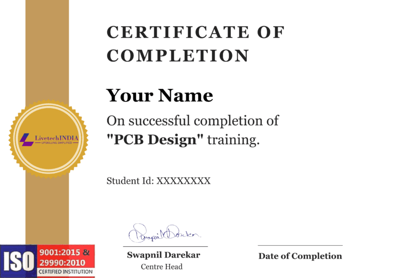
Yes. Upon completion of your training and submission of all projects, you will receive an E-Certificate.
Kindly consult our counselor (9967111302) for details on upcoming Power BI batches. Your session will start immediately upon payment of fees.
The fees are kept nominal, and you have the option to pay in installments. However, if you choose to pay the entire amount upfront, you’ll also receive a further discount. Kindly consult our counselor (Mobile: 9967111302) for details.
We’re an ISO 9001:2008 Certified Training Company based in Andheri and Panvel.
LivetechINDIA has a center in Andheri and Panvel and also team of 25 professionals to cater online trainings across globe.